
WarpStack: resolution on demand
Package warpage and the stress at the corners you name, each at the resolution it needs, in one run on a single desktop.
Warpage is a whole-package quantity, and it settles on a coarse mesh; white paper No. 01 shows it. Stress is not. It concentrates at die corners and gaps a few tens of microns across, and a coarse mesh averages it away. Resolution on demand lets you name the critical regions and the resolution you need there (50 µm, 10 µm) and returns the package warpage and those regions' stresses together. On a production-class AMD MI350-class package it delivers 10 µm at five critical corners in 5.4 minutes on a single desktop, where a uniform 10 µm mesh is projected at 2.9 billion degrees of freedom and ~25 TB of memory. Warpage matches the converged reference to 0.2%; the peak corner stress rises 5.6× over what the coarse mesh reports.
Warpage settles early. Stress does not.
A package bows over tens of millimetres; a die corner concentrates stress over tens of microns. One uniform mesh cannot serve both without becoming unaffordable. With resolution on demand you ask for exactly what each question needs: the package at the resolution where warpage has converged, and 50 µm or 10 µm at the corners and gaps you name, in one run, in minutes.
The package and the request
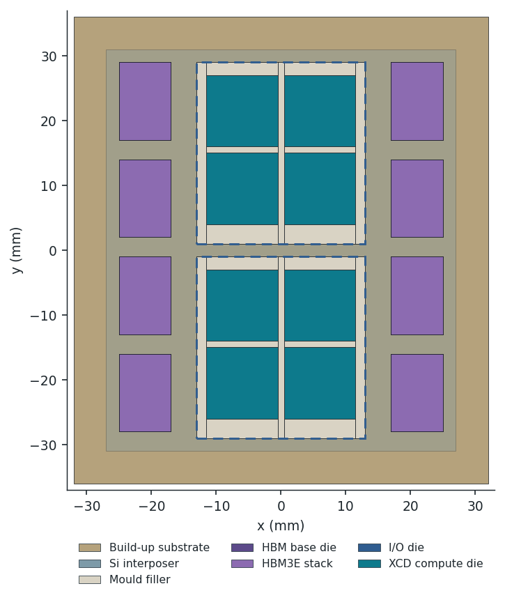
AMD MI350-class: 8 compute dies, 2 I/O dies, 8 HBM3E stacks, 5 critical regions. The same package as white paper No. 01.
| Parameter | Value |
|---|---|
| Package | 64 × 72 mm |
| Mechanical layers | 457 |
| Thermal load | 200 → 85 °C |
| Package resolution | 380 µm · 2.4 M DOF |
| Requested resolution | 50 µm and 10 µm |
| Critical regions | Substrate, interposer, HBM-stack and compute-die corners; the gap between the I/O dies |
What it cost
One desktop: package warpage plus all five regions, in minutes.
| Requested resolution | Wall time | Peak memory |
|---|---|---|
| 50 µm at 5 regions | 4.1 min | 27 GB |
| 10 µm at 5 regions | 5.4 min | 27 GB |
Wall time covers the whole job: the full-package warpage and every requested region, with each region's consistency with the full package verified automatically. Hardware is a single NVIDIA GB10 desktop, not a cluster.
Warpage
| Peak-to-peak | Value |
|---|---|
| This run | 1838.5 µm |
| Converged fine-mesh reference | 1842.7 µm |
| Difference | 0.2% |
The warpage answer is already in hand at package resolution. Going to 10 µm in the critical regions changes local surface shape by about 1 µm; warpage did not need the fine mesh. Stress does.
Why the resolution still matters
Peak interface stress, coarse vs requested.
At 50 µm: 1 mm critical regions, MPa, up to 1.7×
| Region | Package mesh | 50 µm |
|---|---|---|
| Compute-die / I/O-die corner | 185 | 228 |
| Gap between the I/O dies | 36 | 62 |
| HBM-stack corner | 38 | 47 |
| Interposer corner | 34 | 47 |
| Substrate corner | <0.1 | <0.1 |
At 10 µm: 0.4 mm critical regions, MPa, up to 5.6×
| Region | Package mesh | 10 µm |
|---|---|---|
| Compute-die / I/O-die corner | 84 | 472 |
| Gap between the I/O dies | 16 | 9 |
| HBM-stack corner | 27 | 57 |
| Interposer corner | 30 | 74 |
| Substrate corner | <0.1 | <0.1 |
Each table compares like with like: the package-mesh value and the refined value over the same region. The 10 µm regions are smaller than the 50 µm ones, so their package-mesh values differ between the two tables. Read the ratio in each row. At 10 µm the compute-die corner stress is 5.6× what the package mesh reports, the interposer corner 2.5× and the HBM-stack corner 2.1×. Resolution also removes false alarms: the gap between the I/O dies comes in lower at 10 µm than the coarse mesh suggests.
What a uniform mesh would have cost
The same resolution everywhere, projected from the structure of the mesh and not solved.
| Approach | Degrees of freedom | Memory | Wall time |
|---|---|---|---|
| Uniform 50 µm mesh (projected) | 116 M | ≈1.0 TB | ≈76 h |
| Uniform 10 µm mesh (projected) | 2.9 B | ≈25 TB | ≈3,600 h · 5 months |
| WarpStack, 50 µm on demand (measured) | 2.4 M + regions | 27 GB | 4.1 min |
| WarpStack, 10 µm on demand (measured) | 2.4 M + regions | 27 GB | 5.4 min |
A uniform 50 µm mesh needs about a terabyte and three days; a uniform 10 µm mesh needs roughly 1,000× the memory this run used, some 200× what the desktop even holds, and about five months. Resolution on demand delivered both resolutions in minutes, in 27 GB. The uniform rows are projections, not results; they were never solved, because no single machine on hand could hold them.
What this buys you
One run, both answers. Package warpage at the resolution where it has converged, and the stress at every corner and gap you care about at the resolution you ask for (50 µm, 10 µm), in minutes on a desktop. The corners that will crack first are seen at the scale they fail at, without paying for that scale across the whole 64 × 72 mm package.
Scope of this study. Same package model as white paper No. 01, solved with the current WarpStack release: a free package body with no board, BGA layer, lid or stiffener, no moisture, cure shrinkage or gravity, and library material properties rather than vendor data. Stresses are linear-elastic peak interface stresses for the 200 → 85 °C load. At a sharp corner where two materials meet, peak stress keeps rising as resolution increases; the compute-die corner value is a severity indicator to be read alongside your design rules, not a converged material stress. Uniform-mesh figures are projections. None of these numbers is a prediction of shipping hardware. AMD, Instinct and MI350 are trademarks of Advanced Micro Devices, Inc. NoveetyAI is not affiliated with, endorsed by, or sponsored by AMD, and this material was not produced in cooperation with AMD.