
Chip, package and board in one model: an MI350-class OAM module
Three design files become one 974 W thermal model, with the hottest compute die resolved at 50 µm on one CPU server.
A GPU module is designed in three tools: the chip stack in 3Dblox, the package and the board in PCB layout tools. ThermStack reads all three design files and builds one thermal model: an MI350-class OAM module at 974 W on a 102 × 165 mm board. ThermStack APR resolves the hottest compute die at 50 µm in 1 h 20 min and 110 GB of memory, on one CPU server.
Three design files, one thermal model
Each level of the module comes in the format its own design team already uses.
| Level | Input file | What it brings |
|---|---|---|
| Board | IPC-2581 | Stack-up, copper on every layer, vias, part placement, VRM stages and their power |
| Package | IPC-2581 | Build-up and core stack-up, copper, microvias and core vias, C4 bumps, BGA balls, capacitors |
| Chip stack | 3Dblox 2.1 + CSV power maps | Interposer, compute and I/O dies, HBM stacks, bonding layers, 10 µm power map on each compute die |
The board file places the package at its GPU site; the package places the chip stack on its top side. ThermStack aligns the three levels, resolves the copper of the board and package layouts, and joins them into a single model with one set of boundary conditions. No hand-built geometry and no manual stack-up entry.
Formats ThermStack reads
| Format | Typical source |
|---|---|
| 3Dblox 1.0–3.0 | Chiplet and 3D-IC stacks |
| GDSII + process stack | Die and interposer layouts, photonic and RF cells |
| IPC-2581 | Package substrates and PCBs |
| ODB++ | Package substrates and PCBs |
| Allegro .brd / .mcm / .sip | Through an IPC-2581 or ODB++ export |
| ECXML (JEDEC JEP181) | Thermal models exchanged between tools and suppliers |
| CSV power maps | Per-die power density, static or time-varying |
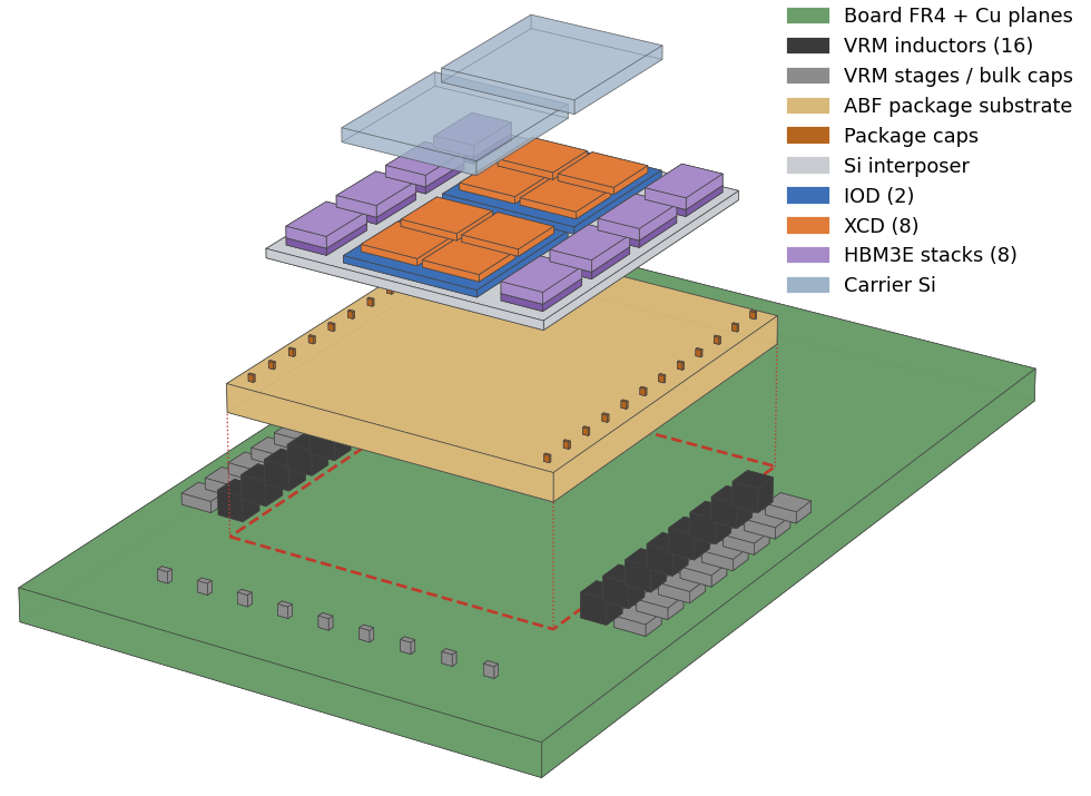
An MI350-class OAM module
The module follows the public outline of an OCP Accelerator Module (OAM) with an MI350-class GPU. All three layouts are synthetic, written for this study.
| Level | Size | Construction | Power |
|---|---|---|---|
| Board | 102 × 165 mm, ~2.0 mm thick | 12 copper layers; 16 VRM stages with inductors and bulk capacitors; dog-bone fan-out and thermal vias under the VRM stages | 24 W (16 × 1.5 W) |
| Package | 64 × 72 mm, ~0.96 mm thick | 5-2-5 ABF build-up, 12 copper layers; 83,700 C4 bumps; 4,608 BGA balls; capacitors on the top side | — |
| Chip stack | 54 × 62 mm interposer | 8 compute dies (XCD), 2 I/O dies (IOD), 8 HBM3E 12-high stacks, carrier silicon | 950 W |
Cooling: cold plate on the module footprint (10,000 W/m²K); 10 W/m²K on the rest of the board top and 50 W/m²K under the board; ambient 25 °C.
50 µm on the hottest compute die, with the whole module in the model
The board, the package and all eight compute dies stay in one model; resolution goes where the hot spots are.
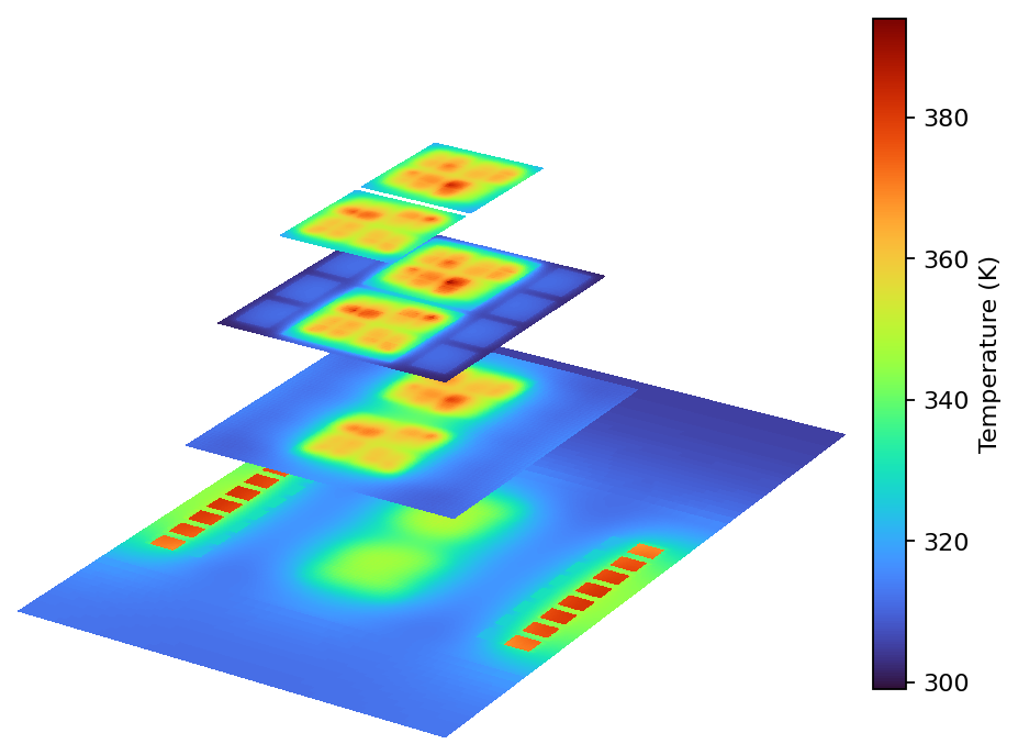
Where the heat goes
The cold plate removes 98.5 % of the 974 W; 1.5 % (14.5 W) leaves through the board. Small as it is, the board still matters. The VRM stages reach about 382 K at 1.5 W each, on board cooling alone, within 13 K of the compute dies; only a model that includes the board shows them. And the module runs cooler than the chip stack alone: modelled on its own, with a plain substrate and the cold plate on the stack, at the same resolution, XCD_6 reads 6.8 K hotter, because the package spreads heat under the cold plate.
MI350-class module with synthetic layouts and power maps, not AMD data. Steady state. Wall time and memory from one 2026 CPU server; they will differ on other hardware. AMD, Instinct and MI350 are trademarks of Advanced Micro Devices, Inc. NoveetyAI is not affiliated with, endorsed by, or sponsored by AMD, and this material was not produced in cooperation with AMD.